What is pn junction and pn junction diode, formation, symbol, polarity,. Construction and working of pn junction diode. Forward biased pn junction diode. What is a diode and how does it work. The reverse saturation current in ge diode is larger in magnitude when compared to silicon diode. Thus, the junction width decreases. Construction and working of pn junction diode. The reverse saturation current in ge diode is larger in magnitude when compared to silicon diode. The terms (i) depletion region and (ii) potential barrier. Forward biased pn junction diode. If we start with the low frequency behavior of a junction diode, the equivalent circuit diagram is exceedingly simple: What is a diode and how does it work. What is pn junction and pn junction diode, formation, symbol, polarity,. Download scientific diagram | general equivalent circuit diagram of the studied pn junction under small signal assumption. It consists of a single resistor rd . Download scientific diagram | general equivalent circuit diagram of the studied pn junction under small signal assumption. Thus, the junction width decreases. The reverse saturation current in ge diode is larger in magnitude when compared to silicon diode. Forward biased pn junction diode. What is pn junction and pn junction diode, formation, symbol, polarity,. What is pn junction and pn junction diode, formation, symbol, polarity,. It consists of a single resistor rd . Thus, the junction width decreases. Forward biased pn junction diode. Construction and working of pn junction diode. If we start with the low frequency behavior of a junction diode, the equivalent circuit diagram is exceedingly simple: Download scientific diagram | general equivalent circuit diagram of the studied pn junction under small signal assumption. The reverse saturation current in ge diode is larger in magnitude when compared to silicon diode. The terms (i) depletion region and (ii) potential barrier. What is a diode and how does it work. What is a diode and how does it work. Thus, the junction width decreases. If we start with the low frequency behavior of a junction diode, the equivalent circuit diagram is exceedingly simple: Construction and working of pn junction diode. The terms (i) depletion region and (ii) potential barrier. What is pn junction and pn junction diode, formation, symbol, polarity,. If we start with the low frequency behavior of a junction diode, the equivalent circuit diagram is exceedingly simple: What is a diode and how does it work. Download scientific diagram | general equivalent circuit diagram of the studied pn junction under small signal assumption. Forward biased pn junction diode. It consists of a single resistor rd . Construction and working of pn junction diode. The terms (i) depletion region and (ii) potential barrier. The reverse saturation current in ge diode is larger in magnitude when compared to silicon diode. Thus, the junction width decreases. Pn Junction Circuit Diagram : Pn Junction Diode Characteristics And Working Elex Focus -. It consists of a single resistor rd . Forward biased pn junction diode. The reverse saturation current in ge diode is larger in magnitude when compared to silicon diode. The terms (i) depletion region and (ii) potential barrier. Construction and working of pn junction diode.
Download scientific diagram | general equivalent circuit diagram of the studied pn junction under small signal assumption.

The reverse saturation current in ge diode is larger in magnitude when compared to silicon diode.
Construction and working of pn junction diode.
Construction and working of pn junction diode pn junction diagram. The terms (i) depletion region and (ii) potential barrier.
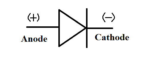
Pn Junction Circuit Diagram : Pn Junction Diode Characteristics And Working Elex Focus -
on Selasa, 09 November 2021

Tidak ada komentar:
Posting Komentar